
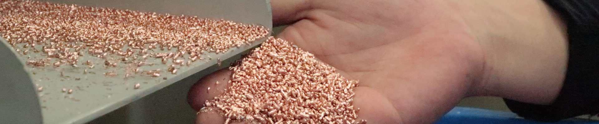
E-waste PCB Dismantling and Recycling Facility
1. What Is E-waste and What Are Waste PCBs?
With the increasing use of electronic devices, e-waste PCB dismantling and recycling facilities have become important for recovering valuable metals and reducing electronic waste. E-waste refers to discarded electrical and electronic equipment, including computers, laptops, mobile phones, televisions, printers, and household appliances.
Printed circuit boards (PCBs) are essential components of many electronic products. They contain electronic components, copper circuits, fiberglass, resin, and small quantities of precious metals. Depending on their source, waste PCBs may contain copper, gold, silver, palladium, and other recoverable materials.
Common types of e-waste processed by recycling facilities include:
- Computer and server PCBs: Motherboards, memory boards, and expansion cards.
- Mobile phone PCBs: Compact circuit boards containing valuable metals.
- Household appliance PCBs: Control boards from washing machines, refrigerators, and other appliances.
- Industrial electronic boards: Circuit boards from control systems and electrical equipment.
- Mixed electronic scrap: Discarded electronic devices containing PCBs, wires, plastics, and metal components.
2. How Are E-waste PCBs Dismantled?
PCB dismantling separates circuit boards from electronic products and removes components that require specialized handling. The process helps improve the efficiency of subsequent material recovery.
The main dismantling steps include:
- Manual disassembly: Workers open electronic equipment using appropriate tools and remove the circuit boards.
- Component removal: Batteries, capacitors, cables, connectors, and other removable components are separated according to the equipment design and applicable safety requirements.
- PCB classification: Circuit boards are sorted by type, size, metal content, and processing requirements.
- Reusable component recovery: Functional boards and components may be tested for refurbishment or reuse.
- Preparation for recycling: Non-reusable PCBs are sent to a suitable mechanical processing line or specialized metal recovery facility.
Proper dismantling reduces contamination and allows different material streams to receive appropriate treatment.
3. Complete E-waste PCB Recycling Process
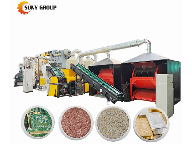
A modern e-waste PCB recycling facility typically combines dismantling, size reduction, mechanical separation, and downstream metal recovery. The exact process depends on PCB composition and the required recovery products.
The typical recycling process includes:
- Collection and sorting: Receive electronic scrap and classify it according to product type and material composition.
- Dismantling and depollution: Remove PCBs from electronic equipment and separate batteries and other hazardous components.
- Shredding and crushing: Reduce suitable PCB materials into smaller particles to release the different material fractions.
- Screening: Separate particles by size to improve the efficiency of subsequent processing.
- Metal separation: Use suitable magnetic, eddy current, electrostatic, or density-based separation technologies, depending on the feed material.
- Dust collection: Install appropriate dust extraction and filtration systems to control airborne particles during mechanical processing.
- Concentrate collection: Collect metal-rich fractions and separate them from fiberglass, resin, and other non-metallic materials.
- Downstream metal recovery: Send suitable concentrates to qualified facilities for further copper and precious metal recovery through specialized metallurgical processes.
Mechanical separation can concentrate valuable metals, but it does not necessarily produce pure gold, silver, or copper directly. Additional refining may be required.
4. What Equipment Is Required for an E-waste PCB Recycling Facility?
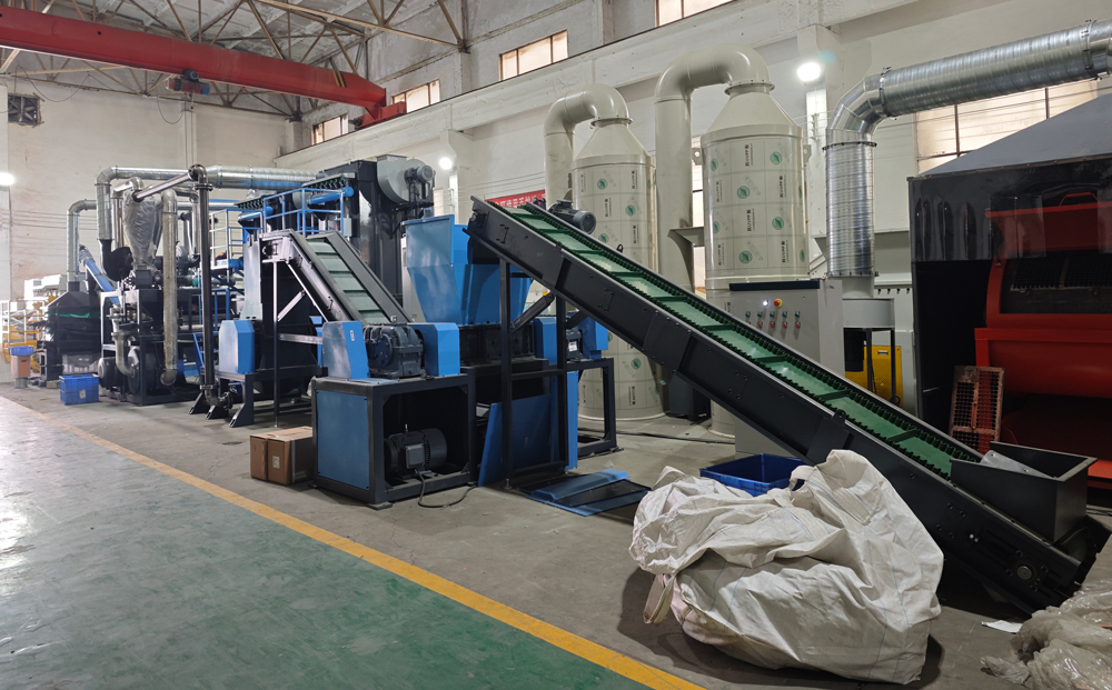
The equipment configuration should match the processing capacity, PCB types, automation requirements, and target material purity.
Common equipment includes:
- PCB dismantling workstations: For opening electronic devices and removing circuit boards.
- PCB component removal machines: For processing suitable boards and separating selected components.
- Double-shaft shredders: For primary size reduction of appropriate electronic scrap.
- PCB crushers and pulverizers: For further size reduction and liberation of material fractions.
- Vibrating screens: For classifying crushed materials by particle size.
- Magnetic separators: For removing ferrous metal contaminants.
- Eddy current separators: For recovering suitable non-ferrous metal fractions.
- Electrostatic separators: For separating conductive metal particles from non-conductive materials where appropriate.
- Dust collection systems: For controlling dust generated during crushing and separation.
- Environmental protection equipment: For managing emissions, wastewater where applicable, and hazardous residues.
A complete facility may also require specialized refining equipment, but hydrometallurgical or smelting systems should be designed and operated separately according to the feed material, process chemistry, and environmental requirements.
5. What Materials Can Be Recovered from Waste PCBs?
An effective PCB recycling system can recover or concentrate several valuable materials:
- Copper: Used in electrical wiring, conductive circuits, and industrial products.
- Gold and silver: Recovered from suitable PCB concentrates through specialized refining.
- Palladium: Present in certain electronic components and recoverable through appropriate downstream processes.
- Iron and aluminum: Recovered from suitable electronic scrap and component fractions.
- Fiberglass and resin: Separated as non-metallic fractions for appropriate treatment or permitted recovery routes.
- Reusable components: Selected electronic parts that pass testing and quality requirements.
Actual recovery rates depend on the PCB grade, metal content, equipment configuration, and downstream refining technology.
6. How to Choose the Right E-waste PCB Recycling Facility?
Before investing in an e-waste PCB dismantling and recycling plant, consider these important factors:
- Processing capacity: Determine the required hourly or daily throughput.
- Raw material composition: Identify whether the facility will process computer boards, mobile phone PCBs, appliance boards, or mixed electronic scrap.
- Recovery efficiency: Evaluate metal recovery performance, separation quality, and final product specifications.
- Automation level: Balance manual dismantling and automated mechanical processing according to labor costs and investment budget.
- Environmental compliance: Plan for dust control, worker protection, hazardous component handling, and local permitting requirements.
- Operating costs: Consider energy consumption, maintenance, labor, spare parts, and downstream refining charges.
E-waste PCB dismantling and recycling facility helps transform discarded electronics into valuable secondary resources. By combining safe dismantling, shredding, screening, mechanical separation, and specialized metal refining, recycling businesses can recover useful materials while reducing waste and environmental risks.
For the best results, choose a customized recycling solution based on PCB composition, processing capacity, recovery targets, and environmental requirements.